10월 4일
FPGA 수업
BASYS3를 사용하며 verilog로 진행한다.
반도체에서 front-end, back-end는 wafer를 기준으로 보면 될 거 같다.
wafer에 설계하는 부분은 back-end.
wafer 전 단계는 front-end.
설계하는 부분은 front-end.
wafer에다가 실제로 chip을 만드는 부분이 back-end.

https://hakucode.tistory.com/27
[Ch. I] Verilog HDL 개요
포스팅에 앞서 이 게시글은 Reference의 contents를 review하는 글임을 밝힌다. Verilog HDL이란? 단순 논리게이트(Logic gate)나 플립플롭(Flip-flop 또는 Latch)에서부터 통신용 모뎀, 멀티미디어 프로세서, 마..
hakucode.tistory.com
반도체 IC 설계
아날로그 설계 - Full custom IC
디지털 설계 - Verilog HDL
VHDL
둘 중 디지털 설계를 배운다.
Gate
http://www.ee.surrey.ac.uk/Projects/CAL/digital-logic/gatesfunc/index.html
Basic Logic Gates
Digital systems are said to be constructed by using logic gates. These gates are the AND, OR, NOT, NAND, NOR, EXOR and EXNOR gates. The basic operations are described below with the aid of truth tables.
www.ee.surrey.ac.uk

전선에 의해 조금씩 전압강하가 일어남. 그래서 일정 길이에 buffer를 달아 전압을 다시 높인다.(교수님은 15cm마다 buffer를 달아야 한다고 말함)
https://www.allaboutcircuits.com/textbook/digital/chpt-3/buffer-gate/
The “Buffer” Gate | Logic Gates | Electronics Textbook
Read about The “Buffer” Gate (Logic Gates ) in our free Electronics Textbook
www.allaboutcircuits.com
예전에는 게이트를 종이에 그리며 했으나, 현대에서는 Verilog 언어를 이용해서 IC 설계. (생산성 up, 시간단축, cost down, 고도화 가능, HLS --> AI 반도체)
---------
Design Specification 사양 설계, 스펙 설계
IC : 무얼 만들 것인가. 입력은? 처리기능(프로세스는 어떻게 할지), 출력은?
-->
Behavioral Modeling 동작 모델링
어떻게 동작을 시킬 것인가. 어떻게 보면 스펙 설계.
-->
RTL level HDL Modeling
이 단계가 Verilog로 코딩하는 단계.
<-->
Functional Simulation
검증. (코딩과 검증을 반복.) //설계부터 상용화까지 대략 1년 정도로 긴데 대부분 코딩과 검증이 오래 걸림.
Placement & Routing
검증이 끝나고 Logic-Sythensis, Gate-level Verification 단계에서 Net list 나옴.
schematic은 하드웨어 설계. net list로 pbc artwork로 넘어가면 배치를 하게 됨. 그게 placement, routing 개념임.
우리는 Logic-Sythensis 단계까지 진행함.
--------
다시 정리
Front-end 설계
- 시스템 사양 설계(Design Specification) 설계
- 행위 수준(Behaviroal Modeling) 모델링, 검증 //UML 그리고 동작을 어떤 식으로 해야겠구나 본 다음 코딩을 했음. UML이 일종의 Behaviroal Modeling이라고 볼 수 있음.
- RTL(Register Transfer Level) 설계 : Verilog 코딩
- Functional Simulation(검증), <timing chart>
- 합성(Logic Sythensis) : 코드가 gate level로 넘어감.
이후 검증들은 더 있으나 여기까지...
Back-end
앞서 설계한 부분에 대한 Net list가 나옴.
- Net list를 바탕으로 layout 설계 : Placement & Routing(P&R)
- Post-layout 검증
- 웨이퍼 칩 제조
-------
package type
DIP
QFP
BGA
---------
74LS00 Pinout


verilog는 확장자가 v로 생김


//verilog
module gates(
input i_switch_0, //한 줄로 써도 됨. input i_switch_0, i_switch_1 가능.
input i_switch_1,
output o_and, o_nand, o_or, o_nor, o_not, o_xor //끝에 아무 것도 안 붙임. 세미콜론도 쉼표도 마침표도 안 씀.
);
assign o_and = i_switch_0 & i_switch_1;
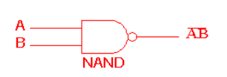
assign o_nand = ~(i_switch_0 & i_switch_1); //~가 비트연산 !는 논리연산
assign o_or = i_switch_0 | i_switch_1;
assign o_nor = ~(i_switch_0 | i_switch_1);
assign o_xor = i_switch_0 ^ i_switch_1;
assign o_not = ~i_switch_0;
endmoduleassign은 연속할당문.
프로그래밍언어와 모델링언어의 가장 큰 차이점은?
Concurrent
Concurrency
"동시성"
(프로그래밍언어는 sequential함.)
그렇기에 하드웨어가 가능함. and 이후에 nor가 작동하는 게 아니라 그냥 전류가 흐르는 대로 작동함. 연속할당문이란 것은 선이 연결됐다고 생각할 수 있음.
[프로그래밍] Concurrency, Parallelism 차이
Concurrency(병행성) 그리고 Parallelism(병렬성) 포스팅 원본출처는 http://egloos.zum.com/minjang/v/2517211 입니다. Concurrency는 프로그램의 성질이고 parallel execution은 기계의 성질이다. Concurrenty..
12bme.tistory.com


https://m.cafe.daum.net/Logic/8LeA/2
test bench란
test bench란 설계한 logic을 simulation할 때 simulation을 원활하게 하기 위해서 작성하는 simulation만을 위한 별도의 code라고 보시면 됩니다. 회로의 simulation입력이 별로 복잡하지 않을..
m.cafe.daum.net
//test용이라서 물리적인 i/o이 필요없음. 괄호 안 씀
module tb_gates();
    reg i_switch_0, i_switch_1;
    wire o_and, o_nand, o_or, o_nor, o_not, o_xor;
    //design under test
    gates dut(
        .i_switch_0(i_switch_0), //.은 매개변수에 할당된 이름. () 안은 입력값
        .i_switch_1(i_switch_1),
        .o_and(o_and),
        .o_nand(o_nand),
        .o_or(o_or),
        .o_nor(o_nor),
        .o_xor(o_xor),
        .o_not(o_not)
    );
    //#은 시간을 의미(nano sec) size'bit
    //sequential하게 동작한다고 봐도 됨. 각각 10 ns 후 다음 동작이 이뤄짐
    initial begin
        #00 i_switch_0 = 1'b0; i_switch_1 = 1'b0;
        #10 i_switch_0 = 1'b0; i_switch_1 = 1'b1;
        #10 i_switch_0 = 1'b1; i_switch_1 = 1'b0;
        #10 i_switch_0 = 1'b1; i_switch_1 = 1'b1;
        #10 $finish;
    end
endmodule
bitstream을 만든 이후 auto connect을 진행한다. 연결이 됐으면 program device를 진행하면 코드대로 실행이 된다.


--------
넥스트칩 라닉스 텔레칩스 엘아이지넥스원


